JMP platforms and statistical methods
Graph Builder:
Histogram, comparative box plots, shape-based heat map
Fit Y by X:
One-way ANOVA, multiple comparisons
Fit Model:
Two-way ANOVA, multiple comparisons
Formula Editor:
Creating new variables
Objective
Use multifactor ANOVA and visualization methods to explore and describe sources of variation in oxide thickness within individual semiconductor wafers, between locations of the wafer within the furnace, and across runs of the process.
Problem statement
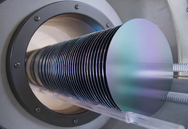
Manufacturing semiconductor wafers involves a process that adds a thin layer of silicon dioxide to wafers. It is done through inserting a set of wafers held in a cartridge (boat) into a thermal reactor (furnace) and slowly adding heat. Once a specified temperature is achieved, a nitrogen oxygen gas mixture is added. This oxidizes the surface of the wafer growing a thin layer of silicon dioxide. Being able to create a uniform thickness of this oxide layer at a desired specification is critical in the fabrication of the final integrated circuits. The specification for this particular process is a thickness of 90 +/- 8 angstroms.
Wafers coming from one production line are having quality issues further downstream in the manufacturing of the circuits. Quality engineers hypothesized that it was a result of non-uniformity in the thickness of the silicon dioxide layer.
To evaluate this hypothesis, a sampling plan was created where wafers were selected from four different fixed locations on the boat (L1, L2, L3, L4) during 12 runs of the process.
The thickness of the oxide layer was measured at 49 different locations on each of the 12 x 4 = 48 wafers using a spectroscopic measurement tool.